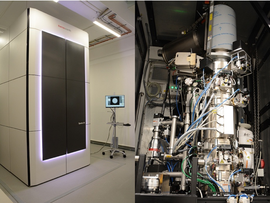
Advanced Transmission Electron Microscopy (TEM) is used to investigate the atomic structure and composition of both nanomaterials and bulk materials, with the latter thinned down to few tens of nanometers. In high-resolution mode (HRTEM), in TEM, a parallel electron beam illuminates an entire region of interest of the sample, creating a two-dimensional projection with a spatial resolution below 2 Å. Additionally, in scanning mode (STEM), the electron beam is focused to a reduced diameter down to 50 pm. Thus, in STEM a converging electron beam is scanned across the sample, and the intensity of electrons scattered at various angles is measured by different detectors. Images are generated by plotting the detector signal at each position during the scan, and hence STEM allows chemical composition analysis through techniques such as Energy-Dispersive X-ray Spectroscopy (EDS) and Electron Energy Loss Spectroscopy (EELS), while electron tomography enables the reconstruction of the sample’s three-dimensional shape.
HRTEM and STEM reveal the atomic structure of the sample projected along the direction of the electron beam, providing information about its crystalline structure, dislocations, and defects. In STEM mode, the use of high-angle annular dark-field (HAADF) electron signal enables element differentiation, as the brightness of an atomic column roughly increases with the square of its average atomic number. When an atom in the sample interacts with the electron beam, it can absorb energy and emit characteristic X-rays. By measuring the energy loss of the beam electrons (EELS spectroscopy) or the energy of the X-rays emitted by the sample (EDS spectroscopy), STEM allows two-dimensional elemental mapping, facilitating the detection of elements even at very low concentrations. Additionally, TEM/STEM with in situ heating or electrical polarization is capable of showing what happens to a sample while it is subjected to a thermal/electrical stimulus.
Reference person: Andrea Falqui